- 您现在的位置:买卖IC网 > Sheet目录3881 > PIC18F8585T-I/PT (Microchip Technology)IC PIC MCU FLASH 24KX16 80TQFP
PIC18F6585/8585/6680/8680
DS30491C-page 254
2004 Microchip Technology Inc.
19.1
A/D Acquisition Requirements
For the A/D converter to meet its specified accuracy,
the charge holding capacitor (CHOLD) must be allowed
to fully charge to the input channel voltage level. The
analog input model is shown in Figure 19-2. The
source impedance (RS) and the internal sampling
switch (RSS) impedance directly affect the time
required to charge the capacitor CHOLD. The sampling
switch (RSS) impedance varies over the device voltage
(VDD). The source impedance affects the offset voltage
at the analog input (due to pin leakage current). The
maximum recommended impedance for analog
sources is 2.5 k
. After the analog input channel is
selected (changed), this acquisition must be done
before the conversion can be started.
To
calculate
the
minimum
acquisition
time,
Equation 19-1 may be used. This equation assumes
that 1/2 LSb error is used (1024 steps for the A/D). The
1/2 LSb error is the maximum error allowed for the A/D
to meet its specified resolution.
Example 19-1 shows the calculation of the minimum
required acquisition time, TACQ. This calculation is based
on the following application system assumptions:
CHOLD
=
120 pF
Rs
=
2.5 k
Conversion Error
≤
1/2 LSb
VDD
=5V
→ Rss = 7 k
Temperature
=
50
°C (system max.)
VHOLD
=
0V @ time = 0
19.2
A/D VREF+ and VREF- References
If external voltage references are used instead of the
internal AVDD and AVSS sources, the source impedance
of the VREF+ and VREF- voltage sources must be consid-
ered. During acquisition, currents supplied by these
sources are insignificant. However, during conversion,
the A/D module sinks and sources current through the
reference sources. The effect of this current, as specified
in parameter A50, along with source impedance must be
considered to meet specified A/D resolution.
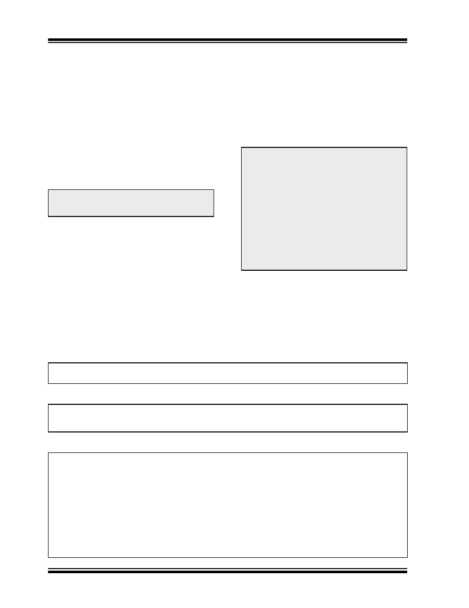
EQUATION 19-1:
ACQUISITION TIME
EQUATION 19-2:
A/D MINIMUM CHARGING TIME
EXAMPLE 19-1:
CALCULATING THE MINIMUM REQUIRED ACQUISITION TIME
Note:
When the conversion is started, the
holding capacitor is disconnected from the
input pin.
Note:
When using external voltage references
with the A/D converter, the source imped-
ance of the external voltage references
must be less than 20
to obtain the spec-
ified A/D resolution. Higher reference
source impedances will increase both
offset and gain errors. Resistive voltage
dividers will not provide a sufficiently low
source impedance.
To maintain the best possible performance
in A/D conversions, external VREF inputs
should be buffered with an operational
amplifier or other low output impedance
circuit.
TACQ
=
Amplifier Settling Time + Holding Capacitor Charging Time + Temperature Coefficient
=TAMP + TC + TCOFF
VHOLD
=
(VREF – (VREF/2048)) (1 – e(-Tc/C
HOLD
(RIC + RSS + RS)))
or
TC
=
-(120 pF)(1 k
+ RSS + RS) ln(1/2047)
TACQ
=TAMP + TC + TCOFF
Temperature coefficient is only required for temperatures > 25
°C.
TACQ
=2
s + TC + [(Temp – 25°C)(0.05 s/°C)]
TC
=-CHOLD (RIC + RSS + RS) ln(1/2047)
-120 pF (1 k
+ 7 k + 2.5 k) ln(0.0004885)
-120 pF (10.5 k
) ln(0.0004885)
-1.26
s (-7.6241)
9.61
s
TACQ
=2
s + 9.61 s + [(50°C – 25°C)(0.05 s/°C)]
11.61
s + 1.25 s
12.86
s
发布紧急采购,3分钟左右您将得到回复。
相关PDF资料
XF2J-2424-11
CONN FPC 24POS 0.5MM SMT
PIC18LF6585T-I/PT
IC PIC MCU FLASH 24KX16 64TQFP
PIC18LF6680T-I/PT
IC PIC MCU FLASH 32KX16 64TQFP
XF2J-2224-11
CONN FPC 22POS 0.5MM SMT
PIC18F6525T-I/PT
IC PIC MCU FLASH 24KX16 64TQFP
PIC18F4439-E/ML
IC PIC MCU FLASH 6KX16 44QFN
XF2J-2024-11
CONN FPC 20POS 0.5MM SMT
PIC16LF747-I/ML
IC PIC MCU FLASH 4KX14 44QFN
相关代理商/技术参数
PIC18F85J10-I/PT
功能描述:8位微控制器 -MCU 32 KB FL 2 KB RAM RoHS:否 制造商:Silicon Labs 核心:8051 处理器系列:C8051F39x 数据总线宽度:8 bit 最大时钟频率:50 MHz 程序存储器大小:16 KB 数据 RAM 大小:1 KB 片上 ADC:Yes 工作电源电压:1.8 V to 3.6 V 工作温度范围:- 40 C to + 105 C 封装 / 箱体:QFN-20 安装风格:SMD/SMT
PIC18F85J10-I/PT
制造商:Microchip Technology Inc 功能描述:IC 8BIT MCU PIC18F 40MHZ TQFP-80 制造商:Microchip Technology Inc 功能描述:IC, 8BIT MCU, PIC18F, 40MHZ, TQFP-80
PIC18F85J10T-I/PT
功能描述:8位微控制器 -MCU 32 KB FL 2 KB RAM RoHS:否 制造商:Silicon Labs 核心:8051 处理器系列:C8051F39x 数据总线宽度:8 bit 最大时钟频率:50 MHz 程序存储器大小:16 KB 数据 RAM 大小:1 KB 片上 ADC:Yes 工作电源电压:1.8 V to 3.6 V 工作温度范围:- 40 C to + 105 C 封装 / 箱体:QFN-20 安装风格:SMD/SMT
PIC18F85J11-I/PT
功能描述:8位微控制器 -MCU 32KB Flash 2048BRAM 67I/O RoHS:否 制造商:Silicon Labs 核心:8051 处理器系列:C8051F39x 数据总线宽度:8 bit 最大时钟频率:50 MHz 程序存储器大小:16 KB 数据 RAM 大小:1 KB 片上 ADC:Yes 工作电源电压:1.8 V to 3.6 V 工作温度范围:- 40 C to + 105 C 封装 / 箱体:QFN-20 安装风格:SMD/SMT
PIC18F85J11T-I/PT
功能描述:8位微控制器 -MCU 32KB Flash 2048bytes-RAM 67I/O RoHS:否 制造商:Silicon Labs 核心:8051 处理器系列:C8051F39x 数据总线宽度:8 bit 最大时钟频率:50 MHz 程序存储器大小:16 KB 数据 RAM 大小:1 KB 片上 ADC:Yes 工作电源电压:1.8 V to 3.6 V 工作温度范围:- 40 C to + 105 C 封装 / 箱体:QFN-20 安装风格:SMD/SMT
PIC18F85J15-I/PT
功能描述:8位微控制器 -MCU 48 KB FL 4 KB RAM RoHS:否 制造商:Silicon Labs 核心:8051 处理器系列:C8051F39x 数据总线宽度:8 bit 最大时钟频率:50 MHz 程序存储器大小:16 KB 数据 RAM 大小:1 KB 片上 ADC:Yes 工作电源电压:1.8 V to 3.6 V 工作温度范围:- 40 C to + 105 C 封装 / 箱体:QFN-20 安装风格:SMD/SMT
PIC18F85J15T-I/PT
功能描述:8位微控制器 -MCU 48 KB FL 4 KB RAM RoHS:否 制造商:Silicon Labs 核心:8051 处理器系列:C8051F39x 数据总线宽度:8 bit 最大时钟频率:50 MHz 程序存储器大小:16 KB 数据 RAM 大小:1 KB 片上 ADC:Yes 工作电源电压:1.8 V to 3.6 V 工作温度范围:- 40 C to + 105 C 封装 / 箱体:QFN-20 安装风格:SMD/SMT
PIC18F85J50-I/PT
功能描述:8位微控制器 -MCU 32KB Flash 3936byte RAM RoHS:否 制造商:Silicon Labs 核心:8051 处理器系列:C8051F39x 数据总线宽度:8 bit 最大时钟频率:50 MHz 程序存储器大小:16 KB 数据 RAM 大小:1 KB 片上 ADC:Yes 工作电源电压:1.8 V to 3.6 V 工作温度范围:- 40 C to + 105 C 封装 / 箱体:QFN-20 安装风格:SMD/SMT